Thus in a Schottky diode the depletion region is not present. Diese Datei und die Informationen unter dem roten Trennstrich werden aus dem zentralen Medienarchiv Wikimedia Commons eingebunden.

Schottky Diode Characteristics Diode Semiconductor Diode Switched Mode Power Supply
Construction of Schottky Diode.

Schottky diodes symbol. Here the anode is the metal side and the cathode is the semiconductor side. 200px 500px 1000px 2000px. Symbol of Schottky diode is shown below.
Brands AP - AZ. It is formed by combining metal with an n-type semiconductor. The symbol of a schottky diode is shown in figure 1.
Brands BA - BZ. P. JIC NFPA Sample Drawing.
Als ein Ergebnis kann die Kombination von groer Wrme mit erhhtem IR Ableitstrom zu einem Anstieg der Gehusetemperatur und der Umgebungstemperatur fhren. Brands CM - CZ. The junction formed between the metal and lightly doped n-type semiconductor.
It has a low forward voltage drop usually 015-045V. Schottky diode uses metals such as tungsten Aluminium chromium platinum gold etc. Schottky diode schematic symbol.
Aus SVG automatisch erzeugte PNG-Grafiken in verschiedenen Auflsungen. As we are aware that in a. In Schottky diode a metal semiconductor junction at one end and another metal semiconductor contact at the other end are formed.
These are generally used in computers and laptops. When doping level of semiconductor is increased then depletion width decreases. The circuit diagram symbol for a Schottky.
Schottky diodes are used where there is a need for limiting losses and high frequency eg in RF applications where there is a need for low forward voltage drop and frequency is also very high. Schottky diode offers fast switching action and has a low forward voltage drop. When the width is.
These diodes are also used for rectification purposes. The figure-4 depicts schottky diode symbol. CCD Diode symbol.
Brands CA - CL. The symbol of the Schottky diode is shown in the figure below. The symbol of Schottky diode given here.
Diodenschemasymbole der elektronischen Schaltung - Diode LED. The schottky diode is a type of metal semiconductor junction diode which is also known as hot-carrier diode low voltage diode or schottky barrier diode. When metal and heavily doped semiconductor contact is present are called Ohmic bilateral contact.
Diode - Schottky Electronic Symbols. Schottky barrier diode circuit symbol Basic Schottky diode characteristics. This is shown in the figure.
The advantages of Schottky diode over Normal PN junction Diode are high switching speed no reverse recovery time. The main application of Schottky diode is high frequency switching application. Schottky diode is also used in the diode.
Brands AA - AO. Schottky diode is not like the previous p n junction diodes. Due to the presence of low voltage drop across the terminals of the diode the Schottky diode is also known as a low voltage diode.
The schottky diode is formed by the junction of a semiconductor with a metal. Disadvantage is low reverse voltage rating. Construction of Schottky Diode.
It uses N-type silicon as semiconductor. Als Konsequenz kann eine falsche thermische Auslegung zu einer Wrmemenge fhren die die abgeleitete Menge bersteigt. Schottky-Dioden sind anfllig fr bermige Wrmeentwicklung whrend hoher Strme.
650V 16A SiC Schottky Diode CoolSiC PG-HDSOP-10-1 DDPAK Keys. Symbol of schottky diode The symbol of schottky diode is shown in the below figure. That is called a unilateral junction.
IEC 60617 Sample Drawing. Zur Beschreibungsseite auf Commons. Brands DA - DZ.
The Schottky diode is a majority carrier device ie. Schottky diode is a special Diode made for the radiofrequency application. In schottky diode the metal acts as the anode and n-type semiconductor acts as.
The junction in a Schottky diode is formed by the metal such as gold tungsten chromium platinum molybdenum or certain silicides and an N-type doped silicon semiconductor. This gives it a significant advantage in terms of speed because it does not rely on holes or electrons recombining when they enter the opposite type of region as in the case of a conventional diode. Electrons in N-type material.
Brands 0 - 9. Also by making the devices small the.

Schottky Diode Electronics Projects Diy Electronics Projects Semiconductor Diode

Photodiode Symbol In 2021 Symbols Circuit Diagram Light Emitting Diode

In5824 Diode Pinout Diode Diodes Tech Company Logos

Main Difference Between Pn Junction Diode And Zener Diode Diode Junction Circuit Diagram

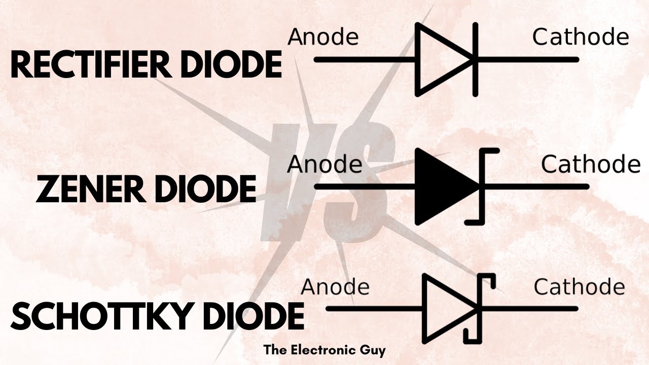
Difference Between Diode Zener Diode And Schottky Diode Diode Different Math

Schottky Diode Circuit Diode Diodes Circuit

Bi Directional Tvs Diode Symbol Diodes Power Electronics Transients
Pin On Diodes

Types Of Diodes And Their Applications 24 Types Of Diodes Diodes Diode Transients

Circuit Symbol Of Diode Diode Zener Diode Tunnel Diode Schottky Diode Light Emitting Diode Led Photodiode Electrical Schematic Symbols Circuit Symbols

Types Of Diodes And Their Applications 24 Types Of Diodes Electronics Basics Cool Electronics Electronics Technology

Types Of Diodes And Their Applications 24 Types Of Diodes Diodes Electronics Basics Diode

Types Of Diodes Electrical Article Diodes Electronics Basics Electronic Circuit Design

Advantages Of Schottky Diode Over Pn Junction Diode Diode Switched Mode Power Supply Semiconductor Materials

Schematic Symbols Diode Electronics Circuit Electronics Basics
Diode Working In A Circuit Diode Diodes Electronics Design

Types Of Diodes And Their Applications 24 Types Of Diodes Diodes Simple Electronics Diode

Gunn Diode Symbol In 2021 Diode Symbols Semiconductor Materials

How To Read A Schematic Electronics Basics Electronic Engineering Electrical Engineering Projects

